
Drive around Silicon Valley and you will see surprisingly little skyline(天际线). The landscape is dotted(点缀,散布) with low-rise offices, bungalows and malls. The microchips that gave the region its name are built in much the same way(以大致相同的方式). Millions of low-rise transistors—the electrical switches which instantiate(实例化,具体体现) a binary 1 or 0, and thus form the basis of computing—are plonked(放下,放置(随意地)) next to each other on a wafer of silicon.
开车绕硅谷转一圈,你会发现天际线低得出奇。风景中点缀着低层办公楼、平房和商场。赋予该地区名字的微芯片的制造方式也大致相同:数百万个低层晶体管——这些电气开关实例化二进制1或0,从而构成计算基础——被随意地并排放置在硅晶圆上。
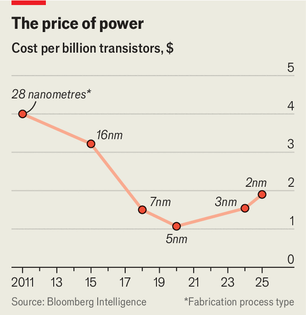
Over the past half-century, in pursuit of(为了追求) higher performance, chipmakers have learned to shrink their transistors and pack them together ever more tightly. But that trick is running out of road(走投无路,不再可行). To keep progress going, firms are starting, at last, to build upwards. The industry’s future will look less like Californian sprawl(蔓延,无计划扩展) and more like the vertical cityscape(城市景观) of Manhattan.
在过去的半个世纪里,为了追求更高性能,芯片制造商学会了缩小晶体管并将它们越来越紧密地打包在一起。但这个把戏已经走不通了。为了保持进步,公司终于开始向上建造。该行业的未来将不再像加利福尼亚的蔓延式发展,而更像曼哈顿的垂直城市景观。
On June 16th, at a conference in Hawaii, Samsung Electronics, a South Korean firm, said it had managed to stack(堆叠) two types of transistor on top of each other, allowing it to make significant savings on space(大幅节省空间). A few days later IBM, an American firm that carries out research into advanced chipmaking, announced a vertical transistor of its own. Intel and TSMC, two other incumbent(现任的,现有的(巨头)) giants, are pursuing similar technology, which the industry hopes may turn up in(出现在) commercial products early in the 2030s.
6月16日,在夏威夷的一次会议上,韩国三星电子表示已成功将两种晶体管堆叠在一起,从而大幅节省空间。几天后,从事先进芯片制造研究的美国IBM公司也宣布了自家的垂直晶体管。英特尔和台积电这两家其他现有巨头也在 pursuing 类似技术,业界希望该技术能在2030年代初出现在商业产品中。
And still I rise
而我依然崛起